Secure DFU OTA for nRF52840 solution modules: Guide to create hex/zip file for implementation – #3(Combining/merging built files)

Following up – Part A: Bootloader (Click for article link) and Part B: Application (Click for article link)

We will be focusing on:

in this article.

IC: nRF52840
DK: PCA10056 (for nRF52840)
SDK: 17.1.0
Softdevice: s140_nrf52_7.2.0_softdevice.hex
IDE: Keil C
PC: Win 10


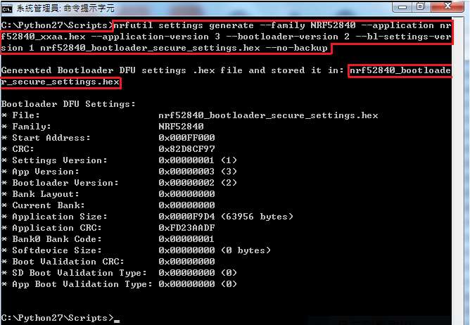
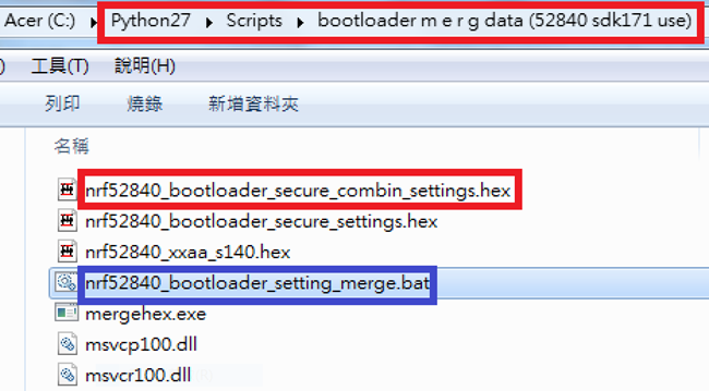
Step 1. Execute the combine batch file in bootloader (nrf52840_bootloader_setting_merge.bat) and generate file of nrf52840_bootloader_secure_combin_settings.hex :

@echo off
title = [ J-Link Tool ] %CD%
set nrfDir=C:\Program Files (x86)\Nordic Semiconductor\nrf5x\bin
set BS= nrf52840_bootloader_secure_settings.hex
set BL= nrf52840_xxaa_s140.hex
set BSBLCombind= nrf52840_bootloader_secure_combin_settings.hex
set path=%nrfDir%;%path%
pause
echo ———–merge image file——————-
mergehex.exe -m %BS% %BL% -o %BSBLCombind%
pause


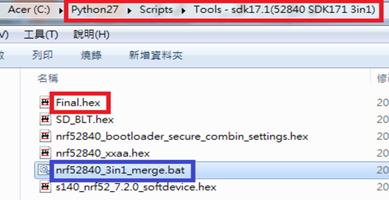
Step 2. Create a Final.hex file by 3-in-1 batch file(nrf52840_3in1_merge.bat)
※Note : This hex file is created for the production line to pre-load firmware into modules prior to shipment.

@echo off
title = [ J-Link Tool ] %CD%
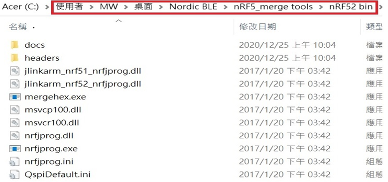
set nrfDir=C:\Users\user\Desktop\Nordic BLE\nRF5_merge tools\nRF52 bin
set SD= s140_nrf52_7.2.0_softdevice.hex
set BLT= nrf52840_bootloader_secure_combin_settings.hex
set APP= nrf52840_xxaa.hex
set SD_BLT=SD_BLT.hex
set Finalfile=Final.hex
set path=%nrfDir%;%path%
pause
echo ———–merge image file——————-
mergehex.exe -m %SD% %BLT% -o %SD_BLT%
pause
mergehex.exe -m %SD_BLT% %APP% -o %Finalfile%
pause


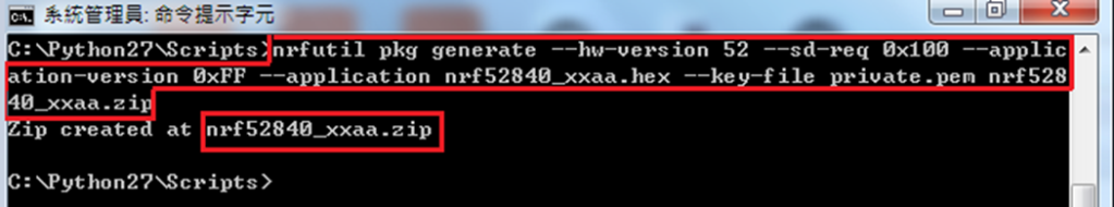
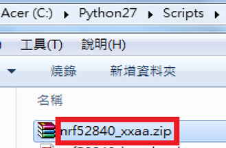
Step 3. Create a DFU(OTA).zip file of nrf52840_xxaa.zip
※Note : This zip file is created for end device DFU(OTA) implementation.

nrfutil pkg generate –hw-version 52 –sd-req 0x100 –application-version 0xFF –application
nrf52840_xxaa.hex –key-file private.pem nrf52840_xxaa.zip
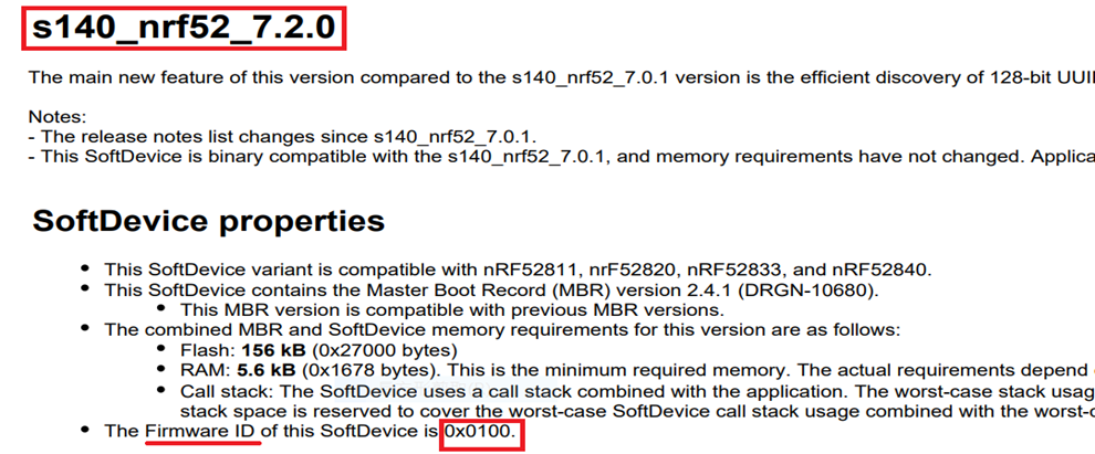
The DFU OTA zip file will be derived.

※Note :
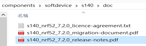
The “0x100" appeared in the above DOS code(in red font) is the FWID(Firmware ID) for s140_nrf52_7.2.0_softdevice.hex;
FWID can be found from the soft device documents on the Nordic website.


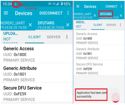
Step 4: Run DFU OTA (On mobile in this example)


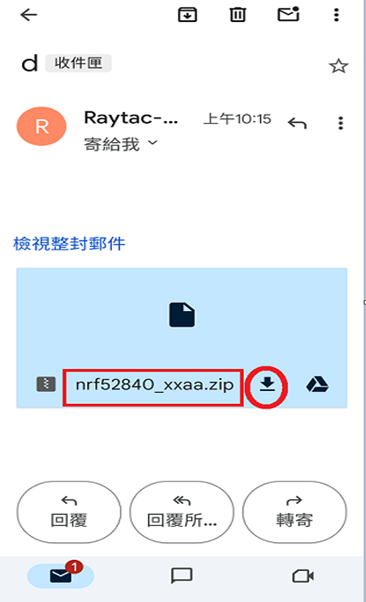
4A. Install the nRF Connect APP on mobile, with DFU OTA file: nrf52840_xxaa.zip. (Download link)


4B. Send nrf52840_xxaa.zip via email to mobile device after combination is done on PC, then download it.


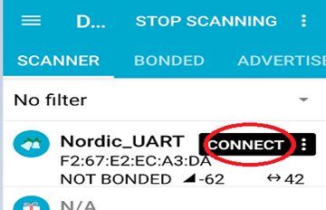
4C. Open nRF Connect APP and run connection;


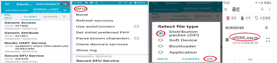
4D. Execute DFU and select “Distribution packet(ZIP)", thus starting the DFU OTA process.


4E. Start DFU OTA → exit the APP after DFU OTA is completed → restart the mobile device.


Secure DFU OTA for nRF52840 solution modules: Guide to create hex/zip file for implementation
Detailed links of articles:
Part A: Bootloader (Click for article link)
Part B: Application
(Click for article link)
Part C: Combining and merging built files
(Click for article link)


Technical guidelines provided by R&D Manager: Mr. MW Lee
Edited by Sales Manager: Mr. Tony Yin

Raytac Corporation 勁達國際電子股份有限公司 
Bluetooth & WiFi module maker based on Nordic nRF54, nRF53, nRF52, nRF7002 solution
BT5.4 &BT5.3 & BT5.2 & BT5.1 Qualified, FCC/IC/CE/Telec/KC/RCM/SRRC/NCC Pre-Certified.
Bluetooth Solution: nRF54, nRF5340, nRF52840, nRF52833, nRF52832, nRF52820, nRF52811, nRF52810, nRF52805, nRF51822
WiFi Solution: nRF7002
http://www.raytac.com
email: service@raytac.com
Tel: +886-2-3234-0208

Secure DFU OTA for nRF52840 solution modules: Guide to create hex/zip file for implementation – #2(Application)

Following up-Part A: Bootloader (Click for article link)

We will be focusing on:

in this article.

IC: nRF52840
DK: PCA10056 (for nRF52840)
SDK: 17.1.0
Softdevice: s140_nrf52_7.2.0_softdevice.hex
IDE: Keil C
PC: Win 10


Path: nRF5_SDK_17.1.0_ddde560\examples\ble_peripheral\ble_app_uart\pca10056\s140\arm5_no_packs

Before building Application code , some amendments need to be made regarding DFU-related settings and code inside Application:

Step 1.


1A. Add code in definition in C/C++ :
BL_SETTINGS_ACCESS_ONLY NRF_DFU_SVCI_ENABLED NRF_DFU_TRANSPORT_BLE=1
(Total 3 steps definitions need to be set up)


1B. Add “include path” in C/C++


1C. Add the .c files inside red frame in (Screenshots 1 & 2)
and the 2 groups of (nRF_DFU & nRF_SVC)(Screenshot 3) under Project(Screenshot 4)


1D. Add code into main.c file in Application (..\examples\ble_peripheral\ble_app_uart\main.c)
(Please refer to: main.c file at: ..\examples\ble_peripheral\ ble_app_buttonless_dfu)


1E. The code of file: sdk_config.h (..\examples\ble_peripheral\ble_app_uart\pca10056\s140\config\
sdk_config.h) inside Application needs to be modified.


1F. Adjust the IRAM1 value in Target after implementing DFU service:
Check on the IRAM1 Value of *p_app_ram_start to be modified from default: 0x20002AE8 0x3D518 to 0x20002AF8 0x3D508, as shown in the red frame in the bottom right corner.
In this case, the program should run successfully.


1G: Create a file of: nrf52840_xxaa.hex after building application code files.


Step 2. Create a bootloader setting file of nrf52840_bootloader_secure_settings.hex : (via DOS)

nrfutil settings generate –family NRF52840 –application nrf52840_xxaa.hex –application-version 3 — bootloader-version 2 –bl-settings-version 1 nrf52840_bootloader_secure_settings.hex –no-backup


※Stay tuned for #3 – Part C: Combining and merging built files in the next article,

scheduled release in next week(05/06/2024).


Technical guidelines provided by R&D Manager: Mr. MW Lee
Edited by Sales Manager: Mr. Tony Yin

Raytac Corporation 勁達國際電子股份有限公司 
Bluetooth & WiFi module maker based on Nordic nRF54, nRF53, nRF52, nRF7002 solution
BT5.4 &BT5.3 & BT5.2 & BT5.1 Qualified, FCC/IC/CE/Telec/KC/RCM/SRRC/NCC Pre-Certified.
Bluetooth Solution: nRF54, nRF5340, nRF52840, nRF52833, nRF52832, nRF52820, nRF52811, nRF52810, nRF52805, nRF51822
WiFi Solution: nRF7002
http://www.raytac.com
email: service@raytac.com
Tel: +886-2-3234-0208

Raytac Product Change Notice (PCN) Announcement for Nordic nRF52840 Solution

Raytac would like to announce Product Change Notice (PCN-19051001) for below Module lines which are built based on Nordic nRF52840 Solution


Correspond to Nordic new revision of the IC with key changes 

(According to Nordic PCN No.: PCN-111 rev. 1.0)


nRF52840 SoC Revision changed from Rev.1 to Rev.2 (Build Code Changed 
from CXX to DXX)

nRF52840 IC Version.png

nRF52840 v.2 – What’s New?

From IC Revision 1 to 2While there are quite a few changes available for review in the nRF52840 documentation, there is update that is particularly important for many users out there, including a large amount of our own customers. The update I am talking about is about the power supply.

First things first – if you’re interested in reading the whole documentation for Nordic Semiconductor’s nRF52840, then look no further than their Infocenter.
nRF52840 IC reversions and variants

As you can see in the picture below, there’s a lot of information about LDO and DC/DC regulators. That is exactly the main topic of today’s post.
On nRF52840 version C, when changing from 5.5V to 3.3V, you had to use LDO mode in order for the chip to function properly. In the new chip version 2, you won’t have to change to LDO mode as you can directly use REG0 DC to DC.

I will let the Infocenter documentation speak for how it works in detail as quoted below:
Nordic Infocenter - nRF52840 Power Supply update.PNG

The system contains two main supply regulator stages, REG0 and REG1.

Each regulator stage has the following regulator type options:

Low-dropout regulator (LDO)
Buck regulator (DC/DC)
In normal voltage mode, only the REG1 regulator stage is used and the REG0 stage is automatically disabled. In high voltage mode, both regulator stages (REG0 and REG1) are used. The output voltage of REG0 can be configured in register REGOUT0. This output voltage is connected to VDD and is the input voltage to REG1.

By default, the LDO regulators are enabled and the DC/DC regulators are disabled. Registers DCDCEN0 and DCDCEN are used to independently enable the DC/DC regulators for the two stages (REG0 and REG1 respectively).

When a DC/DC converter is enabled, the LDO for the corresponding regulator stage will be disabled. External LC filters must be connected for each of the DC/DC regulators being used. The advantage of using a DC/DC regulator is that the overall power consumption is normally reduced as the efficiency of such a regulator is higher than that of a LDO. The efficiency benefit of using a DC/DC regulator becomes particularly prominent when the regulator voltage drop (difference between input and output voltage) is high. The efficiency of internal regulators vary with the supply voltage and the current drawn from the regulators.

Note: Do not enable DC/DC regulator without an external LC filter being connected as this will inhibit device operation, including debug access, until an LC filter is connected.

We hope you get a better understanding about the update from nRF52840 Revision 1 to 2 and its power supply.

Raytac now has started supply module demo board, MDBT50Q-DB, build by nRF52840 v2 SoC.

If you would like to purchase our MDBT50Q-DB demo board (deployed module: MDBT50Q-1MV2) on it, you can get one on eBay or Verical.

We at Raytac wish you all a nice day and happy tinkering 🙂

Raytac Corporation 勁達國際電子有限公司 A BT 5.1 & BT 5 & BT 4.2 module maker based on Nordic nRF51 & nRF52 solution (nRF52840 & nRF52832 & nRF52811 & nRF52810 & nRF51822)

www.raytac.com email: cs@raytac.com Tel: +886.2.3234.0208